Absolute Maximum Ratings (Ta = 25ºC)
| Item | Symbol | Rated value | Unit | |
| Emitter | Forward current | IF | 25 *1 | mA |
| Reverse voltage | VR | 5 | V | |
| Detector | Power supply voltage | VCC | 9 | V |
| Output voltage | VOUT | 17 | V | |
| Output current | IOUT | 8 | mA | |
| Permissible output dissipation | POUT | 80 *1 | mW | |
| Operating temperature | Topr | -30 to +85 *1 | °C | |
| Storage temperature | Pstg | -40 to +90 *1 | °C | |
| Reflow Soldering temperature | Tsol | 255 *2 | °C | |
Electrical and Optical Characteristics (Ta = 25ºC)
| Item | Symbol | Value | Unit
|
Condition | |||
| MIN. | TYP. | MAX. | |||||
| Emitter | Forward voltage | VF | -- | 1.2 | 1.4 | V | IF = 20mA |
| Reverse current | IR | -- | 0.01 | 10 | μA | VR = 5V | |
| Peak emission wavelength | λP | -- | 940 | -- | nm | IF = 20mA | |
| Detector | Power supply voltage | VCC | 2.2 | -- | 7 | V | -- |
| Low-level output voltage | VOL | -- | 0.12 | 0.4 | V | VCC = 2.2 to 7 V, IF = 7 mA, IOL = 8 mA |
|
| High-level output voltage | IOH | -- | -- | 10 | μA | VCC = 2.2 to 7 V, IF = 0 mA, VOH = 17 V |
|
| Current consumption | ICC | -- | 2.8 | 4 | mA | VCC = 7 V | |
| Peak spectral sensitivity wavelength | λP | -- | 870 | -- | nm | VCC = 2.2 to 7 V | |
| LED current when output is ON | IFT | -- | -- | 3.5 | mA | VCC = 2.2 to 7 V | |
| Hysteresis | ΔH | -- | 21 | -- | % | VCC = 2.2 to 7 V | |
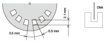
| Response frequency | f | 3 | -- | -- | kHz | VCC = 2.2 to 7 V, IF = 5 mA, IOL = 8 mA *2 |
|
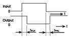
| Response delay time | tPLH | -- | 8 | -- | μs | VCC = 2.2 to 7 V, IF = 5 mA, IOL = 8 mA *2 |
|
| tPHL | -- | 20 | -- | μs | VCC = 2.2 to 7 V, IF = 5 mA, IOL = 8 mA *2 |
||
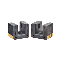
| Connecting method | Weight (g) |
Material |
| Case | ||
| SMT | 0.1 | PPS |
| Document | File Type | File Size | Download |
| EE-SX4320 Datasheet | 1.7 MB |
 |
 |
 |